Interfacing ADC(Analog to Digital Converter) with 8085
Description
Follow the initial 3 steps of interfacing of 8255 with 8085 that are given before.
The ADC 0808 is 8-channel 8-bit ADC chip. It has 8 analog inputs i.e. IN0-IN7.
One of these channels is selected by sending address to a address line of ADC. The logic level and selected channel is as shown:
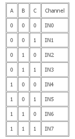 The analog signal is connected to channel 3.
The digital equivalent data D0-D7 is connected to PA0-PA7 of Port A.
The PC0, PC1 and PC2 lines of Port C are connected to channel select address lines of 8255.
PC3 is connected to SOC (Start of conversion) and ALE signal (Input signal). EOC (End of conversion) which is an output signal of 8255 connected to PC7 of Port C.
The PB0 of Port B is connected to OE (Output Enable) input signal of ADC.
The control word format for above interface Is given as:
The analog signal is connected to channel 3.
The digital equivalent data D0-D7 is connected to PA0-PA7 of Port A.
The PC0, PC1 and PC2 lines of Port C are connected to channel select address lines of 8255.
PC3 is connected to SOC (Start of conversion) and ALE signal (Input signal). EOC (End of conversion) which is an output signal of 8255 connected to PC7 of Port C.
The PB0 of Port B is connected to OE (Output Enable) input signal of ADC.
The control word format for above interface Is given as:

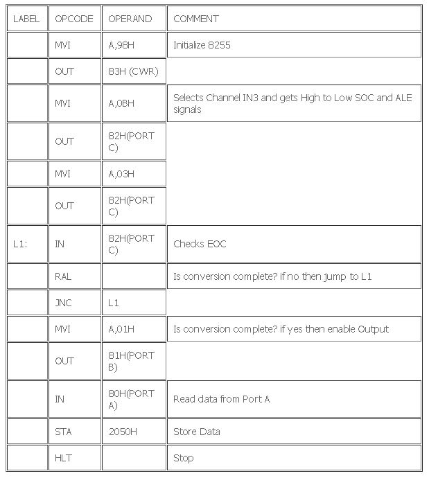
=98H
Data from channel selection: A high to low signal is applied for obtaining data from ADC.
Step 1

=0BH (SOC= HIGH)
Step 2

=03H (SOC= LOW)
OE(Output Enable):

=01H
Program/Code
ADC Interfacing Diagram
 CACKLE comment system


